Signal generator using Si5351 and Arduino NANO
This is a partially working signal generator using Si5351 breakout board and Aduino NANO.
Si5351 came as a breakout board with on board 25 mHz crystal. 8 Khz to 160 mHz was marked on it.
Only CLK0 was used as output.

I don't know how the Si5351 works! So looked for some predigested Si5351 code 😊
Found what I was looking for here
 |
| Si5351 breakout board |

I don't know how the Si5351 works! So looked for some predigested Si5351 code 😊
Found what I was looking for here
Example 4 appeared to be suitable for a simple signal generator.
This is a simple single-file Arduino sketch by Christoph OE1CGS.
This sketch by OE1CGS, is the heart of signal generator sketch.
Signal generator sketch sigGen1.ino and hex file sigGen1.ino.cpp.hex are kept on Google Drive.
Download sigGen1.ino from Google Drive
You may download sigGen1.cpp.hex from Google Drive
The hex file was put in a folder and the following command was executed in that folder..
$ /usr/bin/avrdude -v -patmega328p -carduino -P/dev/ttyUSB0 -b57600 Uflash:w:./sigGen1.cpp.hex:i
hex file uploading tutorial helped me to come up with the above command.
The sketch is repeated here and copy paste should work.
//////////////// Start of sigGen1.ino Line no.1 ////////////////////////////
// Comments are for myself, not for you! ... VU2NIL
#include <Wire.h>
#include <LiquidCrystal.h>
#include <avr/interrupt.h>
#include <avr/sleep.h>
//#define DEBUG // uncomment to activate Serial Monitor
unsigned long int frequency = 10001000;
unsigned long int Step = 10;
/*
PB2, PB3, PB4 and PD3 are used as input, in pin change interrupt mode.
NANO pin D10 PB2 of ATmega328
NANO pin D11 PB3 of ATmega328
NANO pin D12 PB4 of ATmega328
NANO pin D3 PD3 of ATmega328
*/
// digital pins connected to four keys.
const uint8_t tuneUp = 3;
const uint8_t tuneDown = 12;
const uint8_t stepUp = 11;
const uint8_t stepDown = 10;
// flags corresponding to four keys
volatile boolean tu = true;
volatile boolean td = true;
volatile boolean su = true;
volatile boolean sd = true;
/*
Display connections:
<--- 16x2 LCD Display --> Connected to
-LED - Display pin-16 - GND ( MCU/power source)
+LED - Display pin-15 ----1K5 resistor-----+5 Volt
Contrast - Display pin-3 ----2K2 resistor-----GND
VCC - Display pin-2 ----+5 Volt of power source
VSS - Display pin-1 ----GND
R/W - Display pin-5 ----GND
RS - Display pin-4 ----pin9 of NANO -- PB1 of ATmega328
E - Display pin-6 ----pin8 of NANO -- PB0 of ATmega328
DB4 - Display pin-11 ----pin7 of NANO -- PD7 of ATmega328
DB5 - Display pin-12 ----pin6 of NANO -- PD6 of ATmega328
DB6 - Display pin-13 ----pin5 of NANO -- PD5 of ATmega328
DB7 - Display pin-14 ----pin4 of NANO -- PD4 of ATmega328
Lower than 2k2 increases contrast.
*/
// initialize the LCD library with the numbers of the interface pins
LiquidCrystal lcd(9, 8, 7, 6, 5, 4);
void setup()
{
// set up the LCD's number of columns and rows:
lcd.begin(16, 2);
//lcd.cursor(); // turn on the cursor
Wire.begin(); // Initialize I2C-communication as master
// SDA of Si5351 breakout board to pin A4 of NANO
// SCL of Si5351 breakout board to pin A5 of NANO
/* pins connected to four switches are set as input and
are pulled to logic high */
pinMode(tuneUp, INPUT_PULLUP);
pinMode(tuneDown, INPUT_PULLUP);
pinMode(stepUp, INPUT_PULLUP);
pinMode(stepDown, INPUT_PULLUP);
// Pin Change Interrupt setup
noInterrupts(); // disable interrupts
// PCICR - Pin Change Interrupt Control Register
// Pins of port B and port D can be used for pin change interrupt
PCICR = 0b00000101;
// PCMSK0 is Pin Change MaSK register for pins of port B
// PB2, PB3 and PB4 cause interrupt on level change
PCMSK0 = 0b00011100;
// PCMSK2 is Pin Change MaSK register for pins of port D
// PD3 cause interrupt on level change
PCMSK2 = 0b00001000;
interrupts(); // enable interrupts
#ifdef DEBUG
Serial.begin(9600);
#endif
// choose sleep mode
set_sleep_mode(SLEEP_MODE_PWR_DOWN);
lcd.clear(); lcd.setCursor(0,0);
lcd.print("Signal generator");
lcd.setCursor(0,1);
lcd.print("Sleeping ");
} // setup() block end
void loop()
{
// when all keys are inactive go to sleep
if( (tu==true)&&(td==true)&&(su==true)&&(sd==true) ) {
#ifdef DEBUG
Serial.println("Going to sleep!");
delay(200); // allow serial printing to complete
#endif
sleep_enable();
sleep_mode();
#ifdef DEBUG
Serial.println("QRV again!");
#endif
sleep_disable();
}
if ( tu == false ){ // Tune UP block start
if( frequency < 200000000 )
frequency = frequency + Step;
#ifdef DEBUG
Serial.print("Frequency = ");
Serial.println(frequency,DEC);
#endif
SetFrequency (frequency);
lcd.clear(); lcd.setCursor(11,0); lcd.print("Hertz");
lcd.setCursor(0,0); lcd.print(frequency,DEC);
lcd.setCursor(0,1); lcd.print(Step,DEC);
lcd.setCursor(9,1); lcd.print("Hz/STEP");
SetPower(2); TX_ON();
} // Tune UP block end
if ( td == false ) { // Tune Down block start
if ( (frequency > Step) && ( (frequency-Step)>=8000) )
frequency = frequency - Step;
#ifdef DEBUG
Serial.print("Frequency = ");
Serial.println(frequency,DEC);
#endif
SetFrequency (frequency);
lcd.clear(); lcd.setCursor(11,0); lcd.print("Hertz");
lcd.setCursor(0,0); lcd.print(frequency,DEC);
lcd.setCursor(0,1); lcd.print(Step,DEC);
lcd.setCursor(9,1); lcd.print("Hz/STEP");
SetPower(2); TX_ON();
} // Tune Down block end
// Step Up block start
if ( (su == false) && (Step < 10000000) ){
Step = Step*10;
#ifdef DEBUG
Serial.print("STEP = ");
Serial.println(Step,DEC);
#endif
lcd.clear(); lcd.setCursor(0,0); lcd.print("STEP=");
lcd.setCursor(5,0); lcd.print(Step,DEC);
lcd.setCursor(14,0); lcd.print("Hz");
lcd.setCursor(0,1); lcd.print("8kHz to 160mHz ");
delay(1000);
} // Step Up block end
// Step Down block start
if ( (sd == false) && (Step != 1) ) {
Step = Step/10;
#ifdef DEBUG
Serial.print("STEP = ");
Serial.println(Step,DEC);
#endif
lcd.clear(); lcd.setCursor(0,0); lcd.print("STEP=");
lcd.setCursor(5,0); lcd.print(Step,DEC);
lcd.setCursor(14,0); lcd.print("Hz");
lcd.setCursor(0,1); lcd.print("8kHz to 160mHz ");
delay(1000);
} // Step Down block end
delay(200);
if( Step == 1 ) delay(1000);
if( Step == 10 ) delay(500);
} // loop() block end
/* Interrupt Service routine for pin change interrupt on port B.
In this case, the ISR is executed when any of the
Digital pins 10,11 and 12 change level. */
ISR (PCINT0_vect)
{
td = digitalRead (tuneDown);
su = digitalRead (stepUp);
sd = digitalRead (stepDown);
}
/* Interrupt Service routine for pin change interrupt on port D.
In this case, the ISR is executed when
Digital pin 3 change level. */
ISR (PCINT2_vect)
{
tu = digitalRead (tuneUp);
}
/*
Rest of the code is downloaded from here
Minor changes were made to use the code for a signal generator.
Was able to use the code without knowing the innards of Si5351!
The code must be very good ... VU2NIL
*/
/* Line no.352 is commented.
Line no.351 was added.
Next line to line no.333 are commented..... VU2NIL
#include <Wire.h>
void setup() {
Wire.begin(); // Initialize I2C-communication as master
// SDA on pin ADC04
// SCL on pin ADC05
SetFrequency (10140000); // Set TX-Frequency [10,14 MHz]
SetParkMode (); // Initialize park mode
}
void loop() {
TX_ON(); // Switches transmitter on
SetPower(4); // Nothing useful, just changing between different power levels
delay(10000);
SetPower(3);
delay(10000);
SetPower(2);
delay(10000);
SetPower(1);
delay(10000);
TX_OFF(); // Switches transmitter off
}
*/
void TX_ON () { // Enables output on CLK0 and disables Park Mode on CLK1
Si5351a_Write_Reg (17, 128); // Disable output CLK1
Si5351a_Write_Reg (16, 79); // Enable output CLK0, set crystal as source and Integer Mode on PLLA
}
void TX_OFF () { // Disables output on CLK0 and enters Park Mode on CLK1
Si5351a_Write_Reg (16, 128); // Disable output CLK0
Si5351a_Write_Reg (17, 111); // Enable output CLK1, set crystal as source and Integer Mode on PLLB
}
void SetFrequency (unsigned long frequency) { // Frequency in Hz; must be within [7810 Hz to 200 Mhz]
//#define F_XTAL 25000000; // Frequency of XTAL on the Si5351 breakout board ... VU2NIL
#define F_XTAL 25002220; // Corrected frequency ..... VU2NIL
//#define F_XTAL 27005701; // Frequency of Quartz-Oszillator
#define c 1048574; // "c" part of Feedback-Multiplier from XTAL to PLL
unsigned long fvco; // VCO frequency (600-900 MHz) of PLL
unsigned long outdivider; // Output divider in range [4,6,8-900], even numbers preferred
byte R = 1; // Additional Output Divider in range [1,2,4,...128]
byte a; // "a" part of Feedback-Multiplier from XTAL to PLL in range [15,90]
unsigned long b; // "b" part of Feedback-Multiplier from XTAL to PLL
float f; // floating variable, needed in calculation
unsigned long MS0_P1; // Si5351a Output Divider register MS0_P1, P2 and P3 are hardcoded below
unsigned long MSNA_P1; // Si5351a Feedback Multisynth register MSNA_P1
unsigned long MSNA_P2; // Si5351a Feedback Multisynth register MSNA_P2
unsigned long MSNA_P3; // Si5351a Feedback Multisynth register MSNA_P3
outdivider = 900000000 / frequency; // With 900 MHz beeing the maximum internal PLL-Frequency
while (outdivider > 900){ // If output divider out of range (>900) use additional Output divider
R = R * 2;
outdivider = outdivider / 2;
}
if (outdivider % 2) outdivider--; // finds the even divider which delivers the intended Frequency
fvco = outdivider * R * frequency; // Calculate the PLL-Frequency (given the even divider)
switch (R){ // Convert the Output Divider to the bit-setting required in register 44
case 1: R = 0; break; // Bits [6:4] = 000
case 2: R = 16; break; // Bits [6:4] = 001
case 4: R = 32; break; // Bits [6:4] = 010
case 8: R = 48; break; // Bits [6:4] = 011
case 16: R = 64; break; // Bits [6:4] = 100
case 32: R = 80; break; // Bits [6:4] = 101
case 64: R = 96; break; // Bits [6:4] = 110
case 128: R = 112; break; // Bits [6:4] = 111
}
a = fvco / F_XTAL; // Multiplier to get from Quartz-Oscillator Freq. to PLL-Freq.
f = fvco - a * F_XTAL; // Multiplier = a+b/c
f = f * c; // this is just "int" and "float" mathematics
f = f / F_XTAL;
b = f;
MS0_P1 = 128 * outdivider - 512; // Calculation of Output Divider registers MS0_P1 to MS0_P3
// MS0_P2 = 0 and MS0_P3 = 1; these values are hardcoded, see below
f = 128 * b / c; // Calculation of Feedback Multisynth registers MSNA_P1 to MSNA_P3
MSNA_P1 = 128 * a + f - 512;
MSNA_P2 = f;
MSNA_P2 = 128 * b - MSNA_P2 * c;
MSNA_P3 = c;
Si5351a_Write_Reg (16, 128); // Disable output during the following register settings
Si5351a_Write_Reg (26, (MSNA_P3 & 65280) >> 8); // Bits [15:8] of MSNA_P3 in register 26
Si5351a_Write_Reg (27, MSNA_P3 & 255); // Bits [7:0] of MSNA_P3 in register 27
Si5351a_Write_Reg (28, (MSNA_P1 & 196608) >> 16); // Bits [17:16] of MSNA_P1 in bits [1:0] of register 28
Si5351a_Write_Reg (29, (MSNA_P1 & 65280) >> 8); // Bits [15:8] of MSNA_P1 in register 29
Si5351a_Write_Reg (30, MSNA_P1 & 255); // Bits [7:0] of MSNA_P1 in register 30
Si5351a_Write_Reg (31, ((MSNA_P3 & 983040) >> 12) | ((MSNA_P2 & 983040) >> 16)); // Parts of MSNA_P3 and MSNA_P1
Si5351a_Write_Reg (32, (MSNA_P2 & 65280) >> 8); // Bits [15:8] of MSNA_P2 in register 32
Si5351a_Write_Reg (33, MSNA_P2 & 255); // Bits [7:0] of MSNA_P2 in register 33
Si5351a_Write_Reg (42, 0); // Bits [15:8] of MS0_P3 (always 0) in register 42
Si5351a_Write_Reg (43, 1); // Bits [7:0] of MS0_P3 (always 1) in register 43
Si5351a_Write_Reg (44, ((MS0_P1 & 196608) >> 16) | R); // Bits [17:16] of MS0_P1 in bits [1:0] and R in [7:4]
Si5351a_Write_Reg (45, (MS0_P1 & 65280) >> 8); // Bits [15:8] of MS0_P1 in register 45
Si5351a_Write_Reg (46, MS0_P1 & 255); // Bits [7:0] of MS0_P1 in register 46
Si5351a_Write_Reg (47, 0); // Bits [19:16] of MS0_P2 and MS0_P3 are always 0
Si5351a_Write_Reg (48, 0); // Bits [15:8] of MS0_P2 are always 0
Si5351a_Write_Reg (49, 0); // Bits [7:0] of MS0_P2 are always 0
if (outdivider == 4){
Si5351a_Write_Reg (44, 12 | R); // Special settings for R = 4 (see datasheet)
Si5351a_Write_Reg (45, 0); // Bits [15:8] of MS0_P1 must be 0
Si5351a_Write_Reg (46, 0); // Bits [7:0] of MS0_P1 must be 0
}
Si5351a_Write_Reg (177, 32); // This resets PLL A
}
void SetParkMode () { // Sets CLK1 to the Park Mode frequency of 150 MHz to keep the Si5351a warm during key-up
Si5351a_Write_Reg (17, 128); // Disable output during the following register settings
Si5351a_Write_Reg (34, 255); // Bits [15:8] of MSNB_P3
Si5351a_Write_Reg (35, 254); // Bits [7:0] of MSNB_P3
Si5351a_Write_Reg (36, 0); // Bits [17:16] of MSNB_P1 in bits [1:0]
Si5351a_Write_Reg (37, 14); // Bits [15:8] of MSNB_P1
Si5351a_Write_Reg (38, 169); // Bits [7:0] of MSNB_P1
Si5351a_Write_Reg (39, 252); // Parts of MSNB_P3 and MSNB_P1
Si5351a_Write_Reg (40, 130); // Bits [15:8] of MSNB_P2
Si5351a_Write_Reg (41, 82); // Bits [7:0] of MSNB_P2
Si5351a_Write_Reg (50, 0); // Bits [15:8] of MS1_P3
Si5351a_Write_Reg (51, 1); // Bits [7:0] of MS1_P3
Si5351a_Write_Reg (52, 0); // Bits [17:16] of MS1_P1 in bits [1:0] and R in [7:4]
Si5351a_Write_Reg (53, 1); // Bits [15:8] of MS1_P1
Si5351a_Write_Reg (54, 0); // Bits [7:0] of MS1_P1
Si5351a_Write_Reg (55, 0); // Bits [19:16] of MS1_P2 and MS1_P3
Si5351a_Write_Reg (56, 0); // Bits [15:8] of MS1_P2
Si5351a_Write_Reg (57, 0); // Bits [7:0] of MS1_P2
Si5351a_Write_Reg (177, 128); // This resets PLL B
}
void SetPower (byte power){ // Sets the output power level
if (power == 0 || power > 4){power = 0;} // valid power values are 0 (25%), 1 (50%), 2 (75%) or 3 (100%)
switch (power){
case 1:
Si5351a_Write_Reg (16, 76); // CLK0 drive strength = 2mA; power level ~ -8dB
break;
case 2:
Si5351a_Write_Reg (16, 77); // CLK0 drive strength = 4mA; power level ~ -3dB
break;
case 3:
Si5351a_Write_Reg (16, 78); // CLK0 drive strength = 6mA; power level ~ -1dB
break;
case 4:
Si5351a_Write_Reg (16, 79); // CLK0 drive strength = 8mA; power level := 0dB
break;
}
}
void Si5351a_Write_Reg (byte regist, byte value){ // Writes "byte" into "regist" of Si5351a via I2C
Wire.beginTransmission(96); // Starts transmission as master to slave 96, which is the
// I2C address of the Si5351a (see Si5351a datasheet)
Wire.write(regist); // Writes a byte containing the number of the register
Wire.write(value); // Writes a byte containing the value to be written in the register
Wire.endTransmission(); // Sends the data and ends the transmission
}
//////////////// End of sigGen1.ino Line no.472 ////////////////////////////
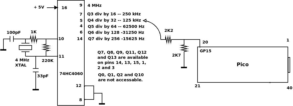
This is the circuit of the Signal generator............

Signal generator schematic
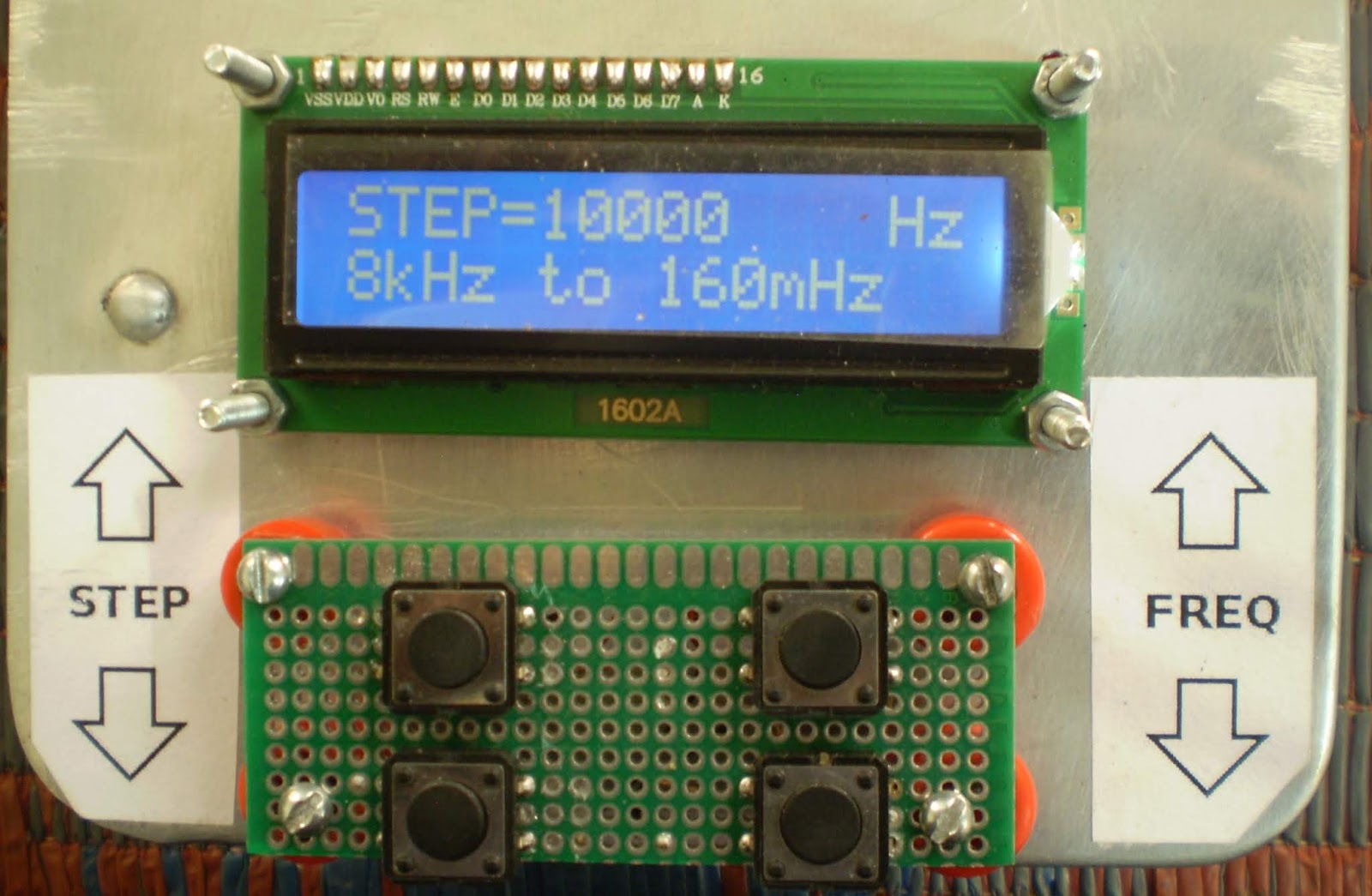
The Signal generator was put on the lid of an small aluminium lunch box.
 |
| Signal generator box |

Signal generator box - inside

Display at power-on
 frequency of this signal generator")

Though 8KHz to 160 mHz was marked on the Si5351 board, 8Khz to a little above 200mHz was tried.
Don't have a standard frequency counter to check the output of Signal generator. HB frequency counter of questionable accuracy has 100 Hz resolution and goes up to about 50mHz. So 8 kHz to 50 mHz could be checked.
Don't have a standard frequency counter to check the output of Signal generator. HB frequency counter of questionable accuracy has 100 Hz resolution and goes up to about 50mHz. So 8 kHz to 50 mHz could be checked.
With VHF radio IC2300H, 136mHz and 174 mHz were checked. Other segments could not be checked😞
Readings with HB RF probe indicated some output at 200mHz. Here is some relative reading.
mHZ mV
50 1490
70 1645
90 2490
110 3160
130 1140
150 402
170 1508
190 245
200 316
I have used a doubtful calibration procedure Don't have the courage to post it!
73 .... VU2NIL
73 .... VU2NIL

Comments
Post a Comment